Thin Film Process Development
E-beam Evaporation and DC Sputtering
Bi-Metal Deposition Optimization | Cr/Au, Ni/Au, Ti/Au, Ni/Cr
🧪 Deposition Methods: E-beam Evaporation (CHA) | DC Magnetron Sputtering (MRC 8667)
🎭 Role: Sole process developer - Designed experiments, optimized parameters, characterized films
Project Overview
This project systematically investigated the deposition of bi-metal thin films using two different physical vapor deposition (PVD) techniques: E-beam evaporation (CHA Evaporator) and DC magnetron sputtering (MRC 8667 Sputterer). Multiple metal combinations including Cr/Au, Ni/Au, Ti/Au, and Ni/Cr were deposited on silicon, PDMS, and glass substrates. The study optimized deposition parameters such as rate, temperature, pressure, and thickness to achieve uniform, adherent films for flexible sensor applications.
Motivation
- Flexible Sensor Metallization: Need for reliable metal contacts on PDMS and other flexible substrates
- Adhesion Optimization: Different substrates require different adhesion layers (Cr, Ti, Ni)
- Process Comparison: Understanding advantages of E-beam vs. Sputtering for different applications
- Runcard Development: Creating standardized process documentation for repeatable fabrication
Equipment Comparison: E-beam vs. Sputtering
| Parameter | E-beam Evaporation (CHA) | DC Magnetron Sputtering (MRC 8667) |
|---|---|---|
| Vacuum Pressure | ~10⁻⁷ Torr (high vacuum) | ~10⁻³ Torr (lower vacuum) |
| Deposition Rate | Controllable (0.1-10 Å/s) | Fixed by power (70-260 Å/min) |
| Film Uniformity | Good (line-of-sight) | Excellent (plasma uniformity) |
| Step Coverage | Poor (directional) | Good (conformal) |
| Film Stress | Lower tensile stress | Higher compressive stress |
| Material Utilization | Low (wasted on chamber walls) | Higher (target erosion) |
Metal Combinations Studied
Cr/Au (Chromium/Gold)
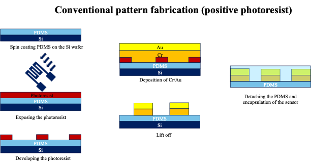
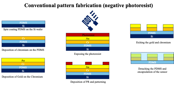
Application: Flexible pressure sensor electrodes, MEMS devices. Cr provides excellent adhesion to PDMS and silicon; Au provides low resistance and oxidation resistance. However, metal deposition requires plasma treatment on the PDMS substrate to achieve wrinkle free metal deposition.
Measured Thickness: Cr = 30.5 nm, Au = 115.7 nm
Ni/Au (Nickel/Gold)
Application: Magnetic sensors, electrodes requiring ferromagnetic properties. Ni provides good adhesion and magnetic functionality. Sputtering creates wrinkle free metal deposition on PDMS substrate without plasma treatment.
Ti/Au (Titanium/Gold)
Application: Biocompatible electrodes, sensors requiring excellent adhesion to oxides. Ti is biocompatible and forms strong bonds with SiO₂.
Ni/Cu (Nickel/Copper)
Process Runcards Developed
Key Findings & Process Insights
1. Substrate Cleaning Criticality
Acetone soak (120 sec) + IPA rinse (60 sec) + DI rinse + SRD (Spin-Rinse-Dryer) pre-programmed recipe. Dehydration bake at 100°C for 60 sec significantly improved adhesion.
2. PMMA Sacrificial Layer Optimization
Spin parameters: 500 rpm (5 sec) → 3000 rpm (30 sec). Bake at 180°C for 60 sec. PMMA enabled clean lift-off for transfer printing applications.
3. PDMS Deposition on Silicon
Spin parameters: 200 rpm (5 sec) → 1000 rpm (50 sec). Cured at 80°C for 12 hours. Achieved uniform PDMS thickness for flexible substrate fabrication.
4. E-beam Evaporation Parameters (CHA)
- Cr (Adhesion): Rate 2Å/s, Target 150Å → Measured 30.5nm
- Au (Conductor): Rate 1.2Å/s, Target 1000Å → Measured 115.7nm
5. Sputtering Parameters (MRC 8667)
- Cu: Rate 70 Å/min, Target 1000Å
- Ni (Sputter): 40 minutes deposition → ~2000nm
6. Lift-Off Process Development
Remover PG soak for 4 hours (until complete). Critical for clean metal patterning on flexible substrates.
Material Characterization
Thickness Measurement (Alpha Step Profilometry):
- Cr layer: 30.5 nm (target 150Å = 15nm → 2× target due to rate variation)
- Au layer: 115.7 nm (target 1000Å = 100nm → close to target)
- Ni (sputter): ~2000 nm (40 min deposition)
Adhesion Testing:
- Cr/Au on PDMS: Excellent adhesion after O₂ plasma treatment
- Ni/Au on Si: Good adhesion, slight cracking at high temperature
- Ti/Au on SiO₂: Excellent adhesion, preferred for oxide substrates
Failure Analysis & Troubleshooting
| Problem | Root Cause | Solution |
|---|---|---|
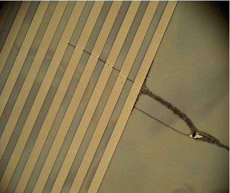
| Metal cracking on PDMS | Thermal expansion mismatch | O₂ plasma treatment before deposition |
| Poor lift-off | Insufficient Remover PG soak | Extended soak to 4 hours |
| Non-uniform film thickness | Substrate positioning in evaporator | Centered substrate placement, substrate rotation |
| Ni adhesion failure | Native oxide on Ni | Immediate Au capping after Ni deposition |
Equipment Used
- CHA E-beam Evaporator
- MRC 8667 DC Magnetron Sputterer
- Headway Spin Coater
- Despatch Oven (PDMS Curing)
- MARCH RIE (O₂ Plasma)
- Alpha Step Profilometer
- Olympus MX150 Microscope
- Spin-Rinse-Dryer (SRD)
- Develop Deck (Wet Processing)
- Solvent Hood (Lift-Off)
Skills Acquired
Applications Enabled
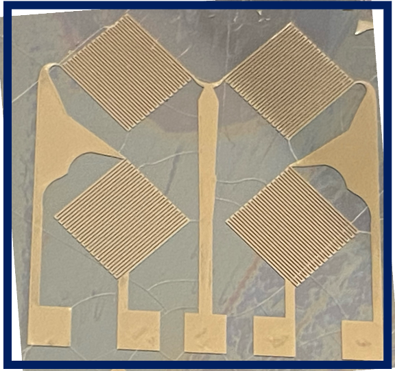
- Flexible Pressure Sensors: Cr/Au on PDMS for stretchable electrodes
- MEMS Devices: Ni/Cr for bridge patterns and resistive elements
- Microsupercapacitors: Cu/Pd for high-conductivity interconnects
- Biosensors: Ti/Au for biocompatible electrode surfaces
Conclusion
This thin film process development project systematically optimized bi-metal deposition using E-beam evaporation and DC magnetron sputtering. Key achievements include: (1) successful Cr/Au deposition on PDMS with measured thicknesses of 30.5 nm Cr and 115.7 nm Au; (2) Ni/Au and Ni/Cr deposition for bridge patterns and magnetic applications; (3) Cu/Pd sputtering for high-conductivity interconnects; (4) development of standardized process runcards for repeatable fabrication; (5) comprehensive comparison of E-beam vs. sputtering for different substrate requirements. The optimized processes directly enabled flexible pressure sensor fabrication, MEMS device metallization, and microsupercapacitor electrode formation. All processes are documented with detailed runcards for technology transfer and repeatability.