SUMMARY
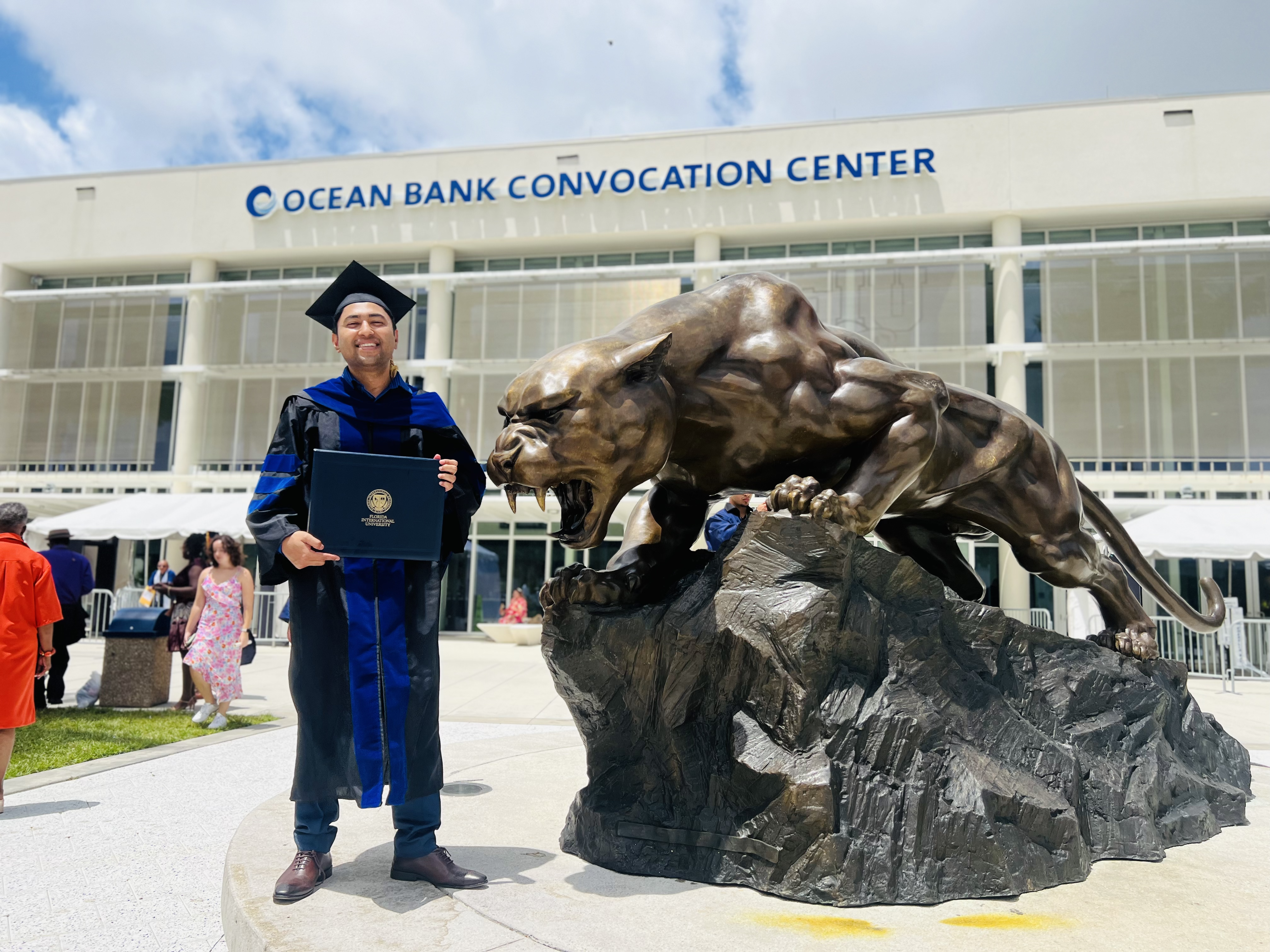
I'm a semiconductor process engineer with a decade of experience across cleanroom fabrication, high-volume manufacturing, and materials science research. I build and optimize processes — from thin-film deposition and photolithography to full device integration — with a focus on yield, reliability, and scalability..
What sets me apart is where I started. Before the cleanroom, I ran shift operations in steel manufacturing and national gas transmission, leading teams and solving problems on systems that couldn't afford to fail. That production mindset shapes everything I do in the lab.
2 U.S. Patents · 10+ Publications · Class 100 Cleanroom · 10 Years of Engineering
If you're looking for a process engineer who combines R&D depth with manufacturing discipline, you're in the right place.